


Process stuck point characteristics
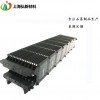
1) Improve product yield: The silicon wafer is firmly clamped, reducing the phenomenon of chip falling, reducing the color difference of silicon nitride, and improving the yield.
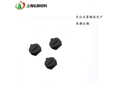
2) The hook point of the process point is small. The hook point area of the new circular process point on the silicon wafer is .472mm2, and the hook point area of the new diamond-shaped process point is 0.619mm2.
3) The service life can reach 90 days
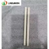
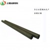
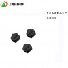
4) Using semiconductor high-purity coated graphite, it has high hardness, wear resistance and long service life.